Camera with PIC32
December 12, 2014
Table of Contents
Project Overview
The goal of this project was to interface the OV7670 camera with the PIC32MX795F512L microcontroller. The camera was chosen based on research while the PIC32 was chosen based on its frequent use at Northwestern.
Microcontroller
The PIC32 was previously used in our Mechatronics classes and was chosen for this project due to its wide use at Northwestern. An Arduino would have been easier; however, Prof. Peshkin wanted a lower level microcontroller. Also, the code to interface the Arduino with the OV7670 can easily be found on the internet. The PIC32 is housed by an NU32 development board. This board also has a serial-to-USB converter which is useful for transmitting data from the camera to my computer. The camera communicates using SCCB (Serial Camera Control Bus); however, SCCB protocol is similar to I2C protocol and therefore I2C communication is used between the microcontroller and the camera. An I2C library was provided by Nick Marchuk for use in our Mechatronics class. The library as well as other downloads helpful for setting up the microcontroller with a computer can be found here in the Full Book Source Code download.
Camera
The OV7670 with FIFO is a cheap CMOS camera. It requires a 3V power supply and is capable of taking 640x480 resolution pictures at up to 30 frames per second.
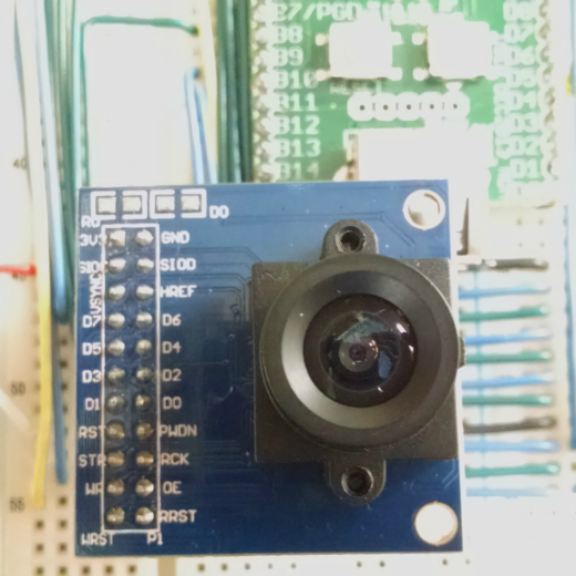
Camera Version
There are many available versions of the OV7670 camera. Some come with an additional AL422 FIFO chip which is helpful for image storage. With the FIFO chip the image can be stored on the chip and then read out later. Otherwise the image needs to be read out at the same time as it is being captured. There are two different versions available of the OV7670 cameras with the AL422 FIFO chip. The version used in this project is the 22 pin version. The most commonly found (and documented) version of the OV7670 camera does not come with the FIFO chip.
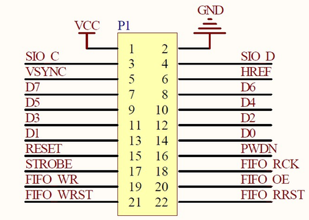
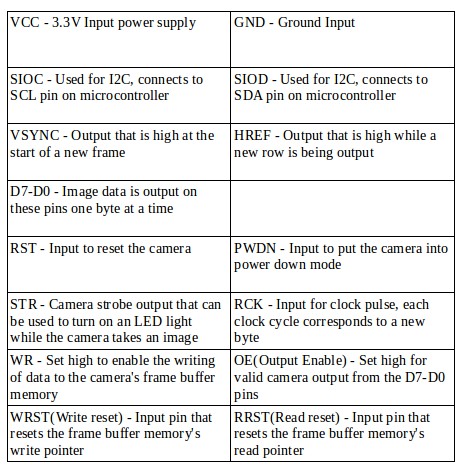
Pin Explanation
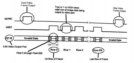
Timing Diagrams
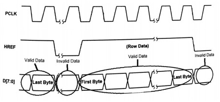
Getting images properly from the camera entirely depends on timing. The following diagrams were taken from Beginning Arduino ov7670 Camera Development. Although the book is written for interfacing the camera with an Arduino microcontroller, it was very helpful in explaining the timing diagrams and giving an outline for the code.
Here is a simple description of what is shown below. VSync will go high at the start of a new frame, then HREF will go high for the start of every row and the pixels for each row will be output from the D7-D0 pins every time PCLK is high. A second high VSync signals the end of a new frame. Parts of the code are explained in the next section and the entire code can be found here.
Steps to Capture Image into Camera’s Frame Buffer Memory
1. Identify when VSync is high - A change notification pin was used to determine when VSync goes high signaling the beginning of a new frame. The initialization of this pin can be found here
void __ISR(_CHANGE_NOTICE_VECTOR, IPL3SOFT) VSyncInterrupt(void) { // INT step 1
	newF = PORTF; // since pins on port F are being monitored by CN,
				  // must read both to allow continued functioning

	read_state = !read_state; //first VSync is beginning of frame
								// and second Vsync is end of frame

	if(read_state){
		reset_write_pointer();
		FIFO_write_enable();
	}

	if(!read_state){
		FIFO_write_disable();
		CNCONbits.ON = 0; // Temporarily turn CN pin off - this is used while debugging
		read_image();
		display_image();
	}

	IFS1bits.CNIF = 0; // clear the interrupt flag
}
2. Reset Write Pointer - Pin E9 (defined as WRST) is used to reset the write pointer so that the image starts saving from the beginning of the frame. The pointer is set low to reset then returned to its original high signal.
void reset_write_pointer(){
	//Reset Write Pointer to 0 which is the beginning of the frame
	//default is high, set pin low to reset
	LATECLR = WRST; //set pin low
	LATESET = WRST; //set pin high
}
3. FIFO Write Enable - Pin E8 (defined as WR) is set high to enable the writing of the image to ram
void FIFO_write_enable(){
	//Set FIFO write enable to active (high) so that image can be written to ram
	LATESET = WR;
}
4. Identify when VSync is high again - The change notification pin just identifies when VSync is high. In order to determine if this is the first trigger or the second trigger I have a read_state variable that will switch back and forth. The memory can only store one image at a time so once the image is read into memory the change notification pin is turned off. Once the image has been displayed the read state variable and the change notification pin can be reset to capture a new image.
read_state = !read_state; //first VSync is beginning of frame
5. FIFO Write Disable - Pin E8 (defined as WR) is set low to enable the writing of the image to ram
void FIFO_write_disable(){
	//Set FIFO write enable to inactive (low) so that image cannot be written to ram
	LATECLR = WR;
}
Steps to Retrieve the Image from the Camera’s Frame Buffer Memory
1. Reset Read Pointer - Pin F0 (defined as RRST) is used to reset the read pointer so that the image starts being output from the beginning of the frame. The pointer is set low to reset then returned to its original high signal.
void reset_read_pointer(){
	//Set the FIFO read buffer pointer to the start of the frame
	//default is high, set pin low to reset
	LATFCLR = RRST; //set pin low
	LATFSET = RRST; //set pin high
}
2. Enable Output - Pin F1 (defined as OE) is set low to enable the output of valid data on the D7-D0 pins.
void FIFO_output_enable(){
	//Set FIFO output enable to active (low) so that image can be read
	LATFCLR = OE;
}
3. Provide Clock Signal - A PWM signal is generated to provide a clock signal for the camera. A new byte is presented onto the D7-D0 pins for every pulse of the clock. The D7-D0 pins on the camera are connected to the B7-B0 pins on the PIC32 and can all be read at once by just reading PORTB.
void rckInitialize(){
T3CONbits.TCKPS = 0; // Timer 3 prescaler N = 1 (1:1), thus it ticks at 80 Mhz (PBCLK/N)
PR3 = FULL_DUTY - 1; // This makes run at 80 Mhz / (N * (PR3+1)) == 10 MHz
TMR3 = 0; // Set the initial timer count to 0
OC1CONbits.OCM = 0b110; // PWM mode without the failsafe for OC1
OC1CONbits.OCTSEL = 1; // use timer 3
OC1RS = FULL_DUTY/2; // Next duty duty cycle is 0
OC1R = FULL_DUTY/2; // Initial duty cycle of 0
T3CONbits.ON = 1; // Turn on timer 3
OC1CONbits.ON = 1; // Turn on output compare 1
}
Camera Registers
Frame Resolution
The OV7670 is capable of outputting images with the following frame resolutions:
- VGA (640x480)
- QVGA (320x240)
- QQVGA (160x120)
- CIF (352x288)
- QCIF (176x144)
These resolutions can be adjusted by setting new values in the Register Set (Table 5 in the Datasheet) The three registers that need to be updated to change the resolution are COM3, COM7, and COM14. Bit 3 in both COM3 and COM14 enable scaling, while bits 5-3 of COM7 are used to pick the specific size. Here is the communication protocol for changing the value in one register.
     i2c_master_start();
     i2c_master_send(0x42); //Write Address
     i2c_master_send(0x0c); //Register Address for COM3
     i2c_master_send(0x00 | 0b00001000); //Default value OR bit you wish to change - this prevents accidentally rewriting over original settings
     i2c_master_stop();
Color Format
The available color formats for this camera are
- YUV/YCrCb
- RGB
- Bayer Raw
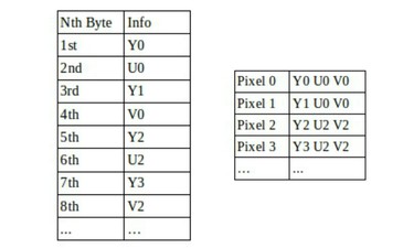
YUV/YCrCb stores brightness value, and red and blue intensity values. The information is outputed as YUYV so every 4 bytes of data corresponds to 2 pixel values, where the U and V information is shared between 2 Ys. YUV can be converted to RGB with a simple formula shown towards the end of this page.
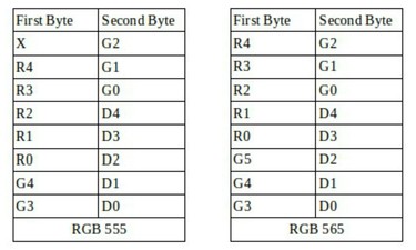
RGB stores information on red, green, and blue components. The information can either be outputted as RGB 888, RGB565, or RGB555. RGB888 is just 3 bytes for every pixel, while the other two compress the information into two bytes per pixel
Bayer Raw is the raw sensor data of either red, green, or blue depending on the color filter at that pixel location.
Changing the color format follows the steps as changing the resolution. The main register that matters when changing color format is COM7 (Bits 2 and 0), but there are many others to control the gains for each color channel.
Test Patterns
In order to test the camera there are a few registers that can be set to produce some test images. The first step is to enable the color bar which is Bit 1 from COM7. After that Bit 7 on both the SCALING_XSC and SCALING_YSC are used to decide between the 8-bar color bar, fade to gray color bar, or no test image. Bits 6 through 0 on both of those registers can be used to control the horizontal and vertical scale factor of the test images.
MATLAB
Reading the image into MATLAB
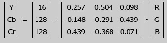
The image data can easily be read from the PIC32 to MATLAB through serial communication. From MATLAB the user has the options of capturing a new frame, dispaying that frame, or toggling between the test patterns. With displaying the frame, the data is first read into MATLAB, then I seperate the data into the Y values and the U/V values. Displaying just the Y values should produce a black and white image. A simple YUV/YCbCr to RGB conversion can be used to see the color image. Each R,G, and B value is then stored individually into an NxNx3 array which can easily be displayed with image(NxNx3 array). A YUV image of [0 128 0 128 0 128 …] is properly converted into an all black image.
Conclusion and Future Work
At the moment the camera often sends plain black images, but does not capture real images. The timing of the provided clock signal, HREF, and reading the bytes has not yet been perfectly aligned to capture an image. An oscilloscope or a logic analyzer can be used to see the timing at such high speeds and debug the timing issue. Once images can be captured the process will need to be automated to stream video. This setup can then be used for many various purposes such as navigation through line following or phototaxis.